
An acupuncture physiotherapy is a home-based physiotherapy device that uses physical therapy at home.
Moxibustion therapy instrument software design instructions
Introduction
Acupuncture therapy is a home-based physiotherapy device that provides health care at home through physiotherapy, primarily by treating the function of the apricot to the human body, making the disease tissue or the whole body better. Modern acupuncture health care has become one of the most important health-care methods.
- 1 The main purpose of this design instruction is to provide the designer concerned with the product with an explanation of the design thinking and code of the control software, thus allowing for the maintenance and further refinement of existing codes and the addition of new functions to the existing ones.
- 2 Project background:
• This project, which is part of a cooperative production research project, deals mainly with software control and integration of acupuncture physiotherapy and creates conditions for the operationalization of acupuncture physiotherapy.
• The software system receives information from blue teeth and regulates it according to human temperature control.
- 3 Specific hardware used in this software:
JDY-08---Bluetooth module
STM32F030 -- Processor used in this software
3P50 - a sensor used in the software
Thermistor
- 4 References:
:: Embedded Product Analysis and Design, Electronic Industry Press, October 2013
ISBN:978-7-121-20618-4
Mission overview
Electronic technology, computer technology and image analysis, are widely used in medicine, physiotherapy equipment. The physiotherapy instrument currently in use is multifunctional, operational, and is also safe and efficient. In foreign countries, home health care and physiotherapy have started early, technology has been improved and popularized, and in recent years physiotherapy has been introduced in the country, and various physiotherapy devices, such as infra-red therapy devices, magnetic field detectors and other small tools, have now entered the home and abroad.
The design uses the Bluetooth module to control the output pulse signal, uses external hardware such as power to form a pulse physiotherapy instrument, and carefully compares the programmes and carefully analyzes the chips used in the design. The system is therefore relatively safe and scalable.
The system software is a collection of programs that do not require user intervention and that also control and coordinate computers and external equipment. The main functions are movement control, monitoring, maintenance of computer systems, and management of independent hardware in computer systems to enable coordination. So it can be said that the software system is a bridge to needs analysis, hardware systems, and the bridge that enables the system to be achieved. The design of the software should first understand the design principles of the software:
- Reliability: Software reliability refers to the ability of the software to avoid failure during the operation of the test, and the ability to escape and the failure to fail after the event.
- Modifications: Reasonable requirements, design of software, good structure, scientific methods for complete documentation, performance of complete systems.
- Easy to adjust, simple program.
- Testability: Testability is the design of an appropriate data set to test the system in place and ensure that it is fully tested.
- Principle of standardization: structurally open up, based on open standards for industry, in line with the norms of the Ministry of State and Information Industry.
Overall design
PWM control part:
Pulse-wided PWM is a term used in a switch-type steady voltage power source. This is classified in the same way as a steady pressure control, except for the PWM type, which is mixed with PFM, PFM and PFM. Pulse-wided (PWM) switch-set steady voltage circuits are designed to stabilize the output voltage by adjusting their space ratio to control the frequency of the circuit's output. With the development of electronic technologies, a variety of PWM technologies have emerged, including: phase voltage control PWM, pulse PWM method, random PWM method, cable voltage control PWM method, etc., while the pulse PWM method, which is used in smart chargers for nickel-hydrogen batteries, is a pulser with an equal width for each pulse as a PWM wave shape, which can be adjusted by changing the cycle of pulses, changing the width or air ratio of pulses, and coordinating the voltage with the frequency using appropriate control methods. Change. The purpose of controlling charged currents can be achieved by adjusting the PWM cycle, the PWM space ratio. The definition of pwm's pulsation system (PWM) is a very effective technique for using microprocessor digital output to control analogue circuits, widely applied in many areas, from measurement, communication to power control and transformation. Similarly, currents absorbed from batteries are not limited to a set of possible values. The difference between analogue signals and digital signals is that the latter ' s values generally fall within a predetermined pool of potential values, such as {0V, 5V}. Simulated voltage and currents can be used directly to control, for example, the volume of the car's radio. In a simple analogue radio, the volume button is connected to a variable electrical resistance. When twisting the switch button, the electrical resistance value becomes larger or smaller; the current flow through this resistance increases or decreases, thereby changing the current value of the drive speaker, making the volume larger or smaller. Like the radio, simulates a linear ratio between the output of the circuit and the input.
While analogue controls may seem intuitive and simple, they are not always very economical or feasible. One of them is that analogue circuits can easily drift over time, making them difficult to regulate. Precise analogue circuits that can solve this problem can be very large, heavy (e.g., old-fashioned home stereo equipment) and expensive. Simulation circuits can also heat heavily, and their power consumption is proportional to the multiplier of both ends of the work component and currents. Simulation circuits can also be sensitive to noise, and any disturbance or noise is bound to change the size of the current value. By numerically controlling analogue circuits, system costs and power consumption can be significantly reduced.
PWM related concepts
The ratio of time spent on high-altitude energy in the output PWM is the ratio of time spent on a PWM clock cycle, like a PWM frequency of 1,000 Hz, which is 1 ms, or 1000us, and if the time of high-altitude is 200us, then the time of low-altitude power is 800us, and the ratio is 200:1,000, which means the ratio of PWM to space is 1:5. The resolution is the minimum of the space ratio, such as 8-bit PWM, the theoretical resolution is 1:255 (single-slash) and the 16-bit PWM theory is 1:655535 (slipper-slash). This is the frequency, such as the 16-bit PWM, which has a resolution of 1:6535. To reach this resolution, T/C must reach from 0 to 65535, if the number starts from 0 to 80 to 80. So the smallest resolution is 1:80, but it's fast, which means that the output of PWM is high. Double / single / single / slope, assuming that a PWM is from 0 to 80, then from 0 to 80. This is a single / slope, assuming that a PWM is from 0 to 80, then from 80 to 0 and then from 80 to 0 and this is a double / slope. As can be seen, the double-slash count has doubled, so the output PWM frequency is half-slow, but the resolution is 1:80 + 80 = 1:160, which is double. Assuming that PWM is a single slope, with a maximum count of 80, we set a comparison value of 10, then T/C will count from 0 to 10 hours (the time count is still up until the count is 80), and the single machine will control whether an IO mouth is output 1 or output 0 at this time or the port is negative.
Analog circuit
The value of the simulated signal can change continuously, without limiting the resolution of the time and range. The 9V battery is an analog assembly because its output voltage does not exactly equal to 9V, but changes over time, and any real value is desirable. Similarly, currents absorbed from the battery are not limited to a set of possible values. The difference between analogue signals and digital signals is that the latter can normally only be taken within a predefined pool of potential values, such as in the collection (0V, 5V). Simulation voltage and currents can be used directly to control, for example, the volume of the car radio. In a simple analogue radio, the volume button is connected to a variable resistance. As with radios, analogue circuit output and input linear proportions. While analogue controls may seem intuitive and simple, they are not always very economical or feasible. One of the things is that analogue circuits can easily drift over time, making it difficult to regulate. Precise analog circuits that can solve this problem can be very large, heavy (e.g. old-fashioned home stereo equipment) and expensive. Simulation circuits can also cause severe heat, and their cost is proportional to the multiplication of the working group's two-end voltage voltage and current. Simulation circuits can also be sensitive to noise, and any disturbance or noise will certainly change the size of the current value.
Digital control
In addition, many microcontrolers and DSPs already contain PWM controllers on chips, making digital control easier to achieve. In short, PWM is a method of digitally coding analogue signals. The PWM signal is still numerical, because at any given time, a full-band direct-flow power is either fully available (ON) or completely non-existent (OFFF). The voltage or current-flow source is added to the simulated load by a repeat pulse sequence (ON) or broken (OFFF). The pass-through is when the direct-flow power is added to the load, and the break is when the power is disconnected.
Hardware controller
Many microcontrollers contain PWM controllers. For example, Microchip’s PIC16C67 contains two PWM controllers, each of which can choose the time and cycle of connection. This microprocessor requires the following work to be done in the software before performing the PWM operation: Set the timer/calculator on the tablet/calculator that provides a changer wave setting the connection time in the PWM control cache setting the direction of the PWM output, which is a universal I/O pipe foot starting the timer enabling the PWM controller, although the specific PWM controller will differ in programming details, but their basic direction is usually the same.
Communication and control
One advantage of PWM is that the signal from the processor to the alleged system is in digital form and does not need a digital simulation. Keep the signal in digital form minimizes the noise impact. Noise can affect a digital signal only if it is strong enough to change logic 1 to logic 0 or logic 0 to logic 1. The shift from analogue signals to PWM can significantly increase communication distance. At the receiving end, the appropriate RC or LC network can filter out high frequency square waves and restore signals to analogue forms. The PWM is widely applied in multiple systems. As a specific example, we look at a brake that is controlled by PWM. In short, a brake is a device that binds something. Many brakes use analogue input signals to control the size of the pressure (or power). The larger the voltage or current on the brake, the greater the pressure on the brake. It is possible to connect the output of the PWM controller to a switch between the power supply and the brake. To generate greater brake power, it is only necessary to increase the percentage of the PWM output by software. If a particular size brake pressure is to be created, it is necessary to determine the mathematical relationship between the space ratio and the pressure by measuring (the formula or search table obtained is used to control temperature, surface wear, etc.). Assuming, for example, that the pressure on the brake is set at 100 psi, the software will do a reverse search to determine what the space ratio for the pressure of this size should be. Then the PWM space ratio is set to this new value, so the brakes can respond accordingly. If there is a sensor in the system, the ratio can be adjusted by a dead-cycle control until the pressure is accurately generated.
Pulse widening (PWM) is a method of digital coding of analogue signals. Through the use of high-resolution counters, the space ratio of square waves is designed to encode the level of a specific simulated signal. The PWM signal is still digital, because at any given time, a full-carrying straight-flow power is either fully available (ON) or completely non-existent (OFF).
Pulse sequences are added to simulated loads. Passage is when direct current power is added to loads, when power is cut off. As long as the bandwidth is sufficient, any analogue can be coded using PWM. Most loads (whether electric or electric loads) require a modulation frequency of more than 10 Hz, usually between 1 kHz and 200 kHz. Many microcontrolers contain PWM controllers. For example, the Microchip PIC16C67 contains two PWM controllers, each of which has the choice of the time and time of connection. The space ratio is the ratio of the time of connection to the cycle; the modem frequency is the penultimate of the cycle. Before the PWM operation, the microprocessor requires that the following be performed in the software:
- Sets the timer/calculator on a piece that provides a modem wave
- Set access time in PWM control repository
- Set the direction of the PWM output, which is a universal I/O tube foot
- Start timer
- Enable PWM controller
One advantage of PWM is that the signal is in digital form from the processor to the system that is charged, and does not need to be converted in numerical terms. Keeping the signal in digital form minimizes the impact of noise. The shift from a simulated signal to a PWM can significantly increase communication distance. At the receiving end, the HF square wave can be filtered out and the signal restored to a simulated form through an appropriate RC or LC network.
There is an important conclusion in the sampling control theory that the effects of narrow pulses of equal impulses and different shapes added to the inertial chain are essentially the same. The PWM control technique is based on this conclusion by controlling the conduct and break of semiconductor switches, so that the output end receives a series of pulses of equal sizes and varying widths, which are used to replace the sine or other wave shapes required. The width of the pulses is regulated by certain rules, which change both the size of the reverse circuit output voltage and the frequency of the output. The rationale for PWM control has long been advanced, but, subject to the level of development of electrical electronics, it was not achieved until the 1980s. Until the early 1980s, with the emergence and rapid development of fully controlled electronics, PWM control technology was not actually applied. With the development of electrical and electronic power, microelectronics and automated control technologies, as well as the application of new theoretical approaches such as modern control theories and the idea of non-linear system control, PWM control technologies have developed unprecedentedly. To date, a variety of PWM control technologies have emerged, based on the characteristics of PWM control technologies.
Pulse-wided PWM is a term used in a switch-type steady voltage power source. This is classified in the same way as a steady pressure control, except for the PWM type, which is mixed with PFM, PFM and PFM. Pulse-wided (PWM) switch-set steady voltage circuits are designed to stabilize the output voltage by adjusting their space ratio to control the frequency of the circuit's output.
Pulse-widening is a very effective technique for the control of analogue circuits using the digital output of microprocessors and is widely applied in many areas, from measurement, communication to power control and conversion.
Pulse width is a mode of simulated control based on the corresponding payload. Changes are made to the bias of the transistor base or MOS grid to effect a change in the timing of transistor or MOS catheters, thereby effecting a change in the output of the switch to the steady voltage source. This way allows the output voltage of the power to remain constant when working conditions change, and is a very effective technique for controlling analogue circuits using microprocessors' digital signals.
The PWM control technology, by virtue of its simple control, flexibility, and dynamic responsiveness, has become the most widely applied control of electricity and electronics, and is a hot spot for research. As today’s advances in science and technology have left no boundaries between disciplines, combining modern control theory or the achievement of unharmonic wave switches will be one of the main directions of PWM’s technology development. It adjusts the bias of the transistor base or MOS grid to the changes in the corresponding load to achieve a change in the timing of transistor or MOS catheters, thereby effecting a change in the output of the switch's steady voltage power source. This allows the output of the power source to remain constant as the working conditions change, and is a very effective technique for controlling analogue circuits using microprocessors' digital signals.
With the development of electronics, a variety of PWM technologies have emerged, including: phase voltage control PWM, pulse PWM method, random PWM method, line voltage control PWM method, etc., while the pulse PWM method, which is used in smart chargers for nickel-hydrogen batteries, is a pulser of equal width per pulse as a PWM wave shape, which can be adjusted by changing the cycle of pulses, changing the width or air ratio of pulses can be adjusted, and the frequency can be coordinated by appropriate control methods. This can be done by adjusting the PWM cycle and the empty ratio of the PWM.
The value of the simulated signal can change continuously, with no limit on the resolution of its time and range. The 9V battery is an emulator because its output voltage does not exactly equal 9V, but changes over time and any real value is desirable. Similarly, currents absorbed from the battery are not limited to a set of possible values. The difference between analogue and digital signals is that the latter ' s extraction value can normally only be in a predetermined pool of potential values, for example {0V, 5V}.
Simulated voltage and currents can be used directly to control, for example, the volume of the car's radio. In a simple analogue radio, the volume button is connected to a variable electrical resistance. When twisting the switch button, the electrical resistance value becomes larger or smaller; the current flow through this resistance increases or decreases, thereby changing the current value of the drive speaker, making the volume larger or smaller. Like the radio, simulates a linear ratio between the output of the circuit and the input.
While analogue controls may seem intuitive and simple, they are not always very economical or feasible. One of them is that analogue circuits can easily drift over time, making them difficult to regulate. Precise analogue circuits that can solve this problem can be very large, heavy (e.g., old-fashioned home stereo equipment) and expensive. Simulation circuits can also heat heavily, and their power consumption is proportional to the multiplier of both ends of the work component and currents. Simulation circuits may also be sensitive to noise, and any disturbance or noise is bound to change the size of the current value.
The cost and utility of the system can be significantly reduced by digital control of analogue circuits. In addition, many microcontrolers and DSPs already contain PWM controllers on chips, which makes digital control easier to achieve.
Working principle of pwm
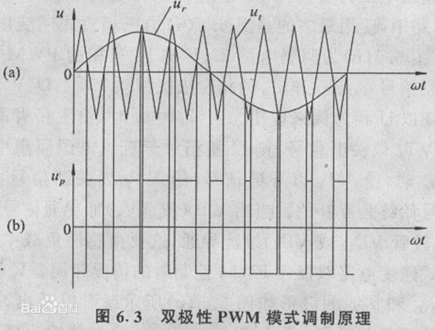
Pulse-wide-modulation waves are usually composed of a column of rectangular pulses with a ratio of space to instant sample values of signals. Figure 1 shows the rationale for pulse-wide-modulation systems.
Box and wave graphs. The system consists of a comparator and a sawytooth generator with a cycle of Ts. The voice signal is larger than the sawytooth signal, and the comparator outputs normal number A or zero. Thus, as can be seen in figure 1, the comparator output drops a column of pulse-wided waves along the modem.
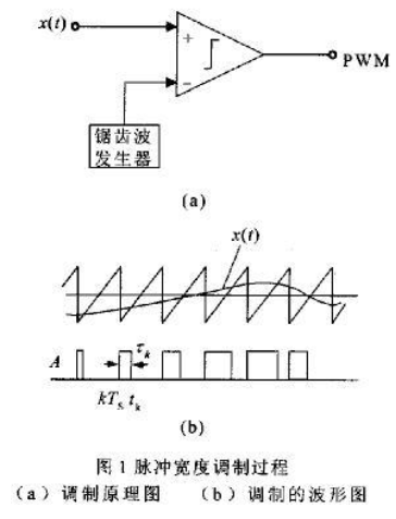
Box and wave graphs. The system consists of a comparator and a sawytooth generator with a cycle of Ts. The voice signal is larger than the sawytooth signal, and the comparator outputs normal number A or zero. Thus, as can be seen in figure 1, the comparator output drops a column of pulse-wided waves along the modem.
As can be seen from the analysis in figure 1b, the width of the rectangular pulse generated depends on the range of the voice signal at the time of the pulse decline. Thus, the time interval between sample values is uneven. The insertion of a sample at the input end of the system to maintain the electrical circuit can provide a uniform sample signal, but in the case of the actual tk-kTs<Ts, the difference between the flat sample and the non-balanced sample is very small. If the sample is assumed to be evenly sampled, the first rectangular pulse can be expressed as:

Where x{t} is a discrete voice signal; Ts
is the sampling cycle; is unmodified width; m is the modem index; however, if the rectangular pulse is approximated as follows: pulse range A, center at t = k Ts
, where the adjacent pulse varies slowly, the pulse width-modulated wavexp(t) can be expressed as:

The pulse width signal can be seen in form (2) by a voice signal x (t) plus a direct flow ingredient and phase-modulated wave structure.
Done. When the signal overlap caused by the phase-modulation component is negligible, the pulse width-modulated wave can be deregulated directly through the low-through filter.
Implementation of digital pulse width modulator:
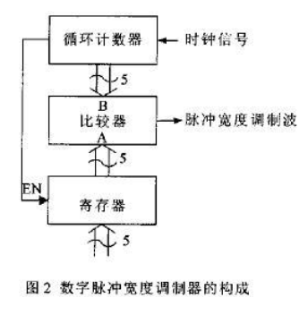
In the figure, the five-bit output of the cycle counter is increased sequentially by the clock pulse. The five-digit moded signal is controlled by a register, continuously compared with the output of the cycle counter, and when the moded signal is larger than the output of the cycle counter, the comparator output high-level or lower-level output. After a cycle, the cycle counter sends an enabling signal to the register, sending the next set of data. In each counter count cycle, due to the size of the moded signals entered, the number of high-level Electro-levels of output from the comparator ' s output ends is different, resulting in the generation of pulse-wide-modulation waves that account for different pulsation ratios.
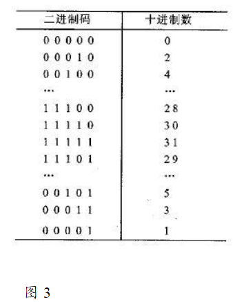
In order to approximate the center of the rectangular pulse at t=kTs, the number code produced by the counter is not a change from small to large or from large to small sequence, but divides the data into even series and odd series, which in one count cycle are smaller and larger, until the maximum value, and then becomes a series of odd numbers, and the change is so large as to be small. The odd sequence is created by using the last of the counters as the lowest level for comparison data, with the lowest level of 0 for the first half of the cycle and an even series for the other heights being increased; the lowest level of 1 for the second half of the period, with the remaining heights decreasing in order, resulting in an even series in descending order. The specific circuit can be shown by the following circuit chart:
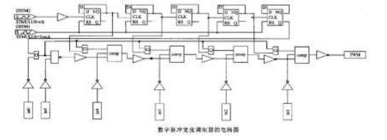
PWM modules should include: 1, Comparable Part (Comp): 2, Count (Counter): 3, Status and Control Signal Repository/Controler (PWM Ctrl); 1) Status Repository: (Flags), Address: E8H; 1EN: PWM module start-up position at „1 ‟ will enable PWM modules to start work; 2 (Screen Standby) 34 modem rate marker position: 00 – no frequency; 01 – 2-minute frequency; 10 – 10-minute frequency; 11 – 16-minute frequency. (RESET = 00 ) 5 (removable reserve) 6 (removable reserve) 7 (removable reserve) 8 (removable reserve) Note: The repository is functional and not readable; it can only be read by by bytes. 2) DataStoree, address: F8H; Note: The memory value is not readable and only written. Port: 1) DataBus (DataBus); 2) Address bus (AddrBus); (IN) 3) PWM wave output port (PWMOut); (OUT) 4) Control Line: 1 CLK: clock; (IN) 2 Reset: Overstep sign; (IN low level effective) 3 WR: write PWM RAM signal; (IN low level effective); 4 RD: Read PWM RAM signal; (IN low-altitude effective)
DONE: Accepts the completed feedback signal (OUT high-altitude effective) 6 INT: Interrupted application signal (OUT low level effective) 7 IntResp: Interrupted response signal (In low level effective) 8 ByteBit: Byte/bit control signal (IN 1-BYTE 0-BIT);
Basic principles of pulse width modulation (PWM):
The control method is to control the breakage of the reverse circuit switch, so that the output end receives a series of pulses of equal value, replacing the sine wave or the wave shape required. That is to say, multiple pulses are generated during half-cycles of the output wave shape, so that the equivalent of the power of the pulse is a swirl shape, and the output is smooth and low-intensity. Adjusting the width of the pulses by certain rules can change the size of the reverse circuit output voltage or the frequency of the output.
For example, by dividing the sine semi-waves into the N equivalent, the sines half-waves can be seen as a waveform consisting of the N-connected pulses. These pulse widths are equal to the thallium/n, but the range varies, and the top of the pulses is not a horizontal line, but a curve, and the bands of the pulses vary according to the sarcophagus. If the aforementioned pulse sequences are replaced by a series of rectangular pulses of the same amount of equal bands and not equal in width, so that the mid-point of the rectangular pulses is reunified with the medium-point of the corresponding sine equivalent, and the rectangular pulses are equal to the area of the corresponding sine part (i.e., the flash amount), a set of pulse sequences, which is the PWM wave shape, can be seen. The pulse widths vary by the sine pattern. According to the principle of the equivalent effect of the flash, the PWM wave and the sine semi-waves are equivalent. For the negative half-week of the sine, the PWM wave shape can be obtained in the same way.
In the PWM wave shape, the band of the pulses is equal, and in order to change the band of the equivalent output sine wave, it is sufficient to change the width of the pulses by the same ratio factor. Thus, in the PWM reverse circuit output, the pulse voltage is the amount of the direct-flow side voltage.
On the basis of the above principles, the width and spacing of the PWM pulses can be calculated precisely after giving the sine wave frequency, the band value and the pulse number in half a cycle. The result of the calculation controls the break-up of the switches in the circuits, and the required PWM wave shape can be obtained.
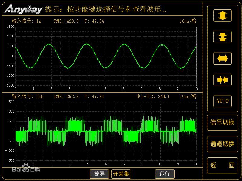
The following figure shows the real-time wave shape of the PWM wave from which the frequency is exported.
PWM(Pulse
Width Modulation Control - Pulse Width Modifier Technology, which achieves the required waveform (with shapes and band values) by adjusting the width of a series of pulses.
The PWM control technology is the most widely used in reverse circuits, most of which are of the PWM type, and it is the application of the PWM control technology in reverse circuits that determines its importance in electrical and electrical technology.
Theoretical basis:
The effect is essentially the same when the narrow pulses of equal impulses and different shapes are added to the inertial chain. The effect is the size of the narrow pulse. The effect is essentially the same, meaning that the output-response wave shape of the chain is essentially the same. The low-frequency segment is very close, with only slight variations in the high-frequency segment.
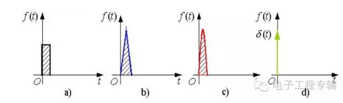
Figure 1 All narrow pulses with different shapes and same impulses
Area equivalent principle:
The effect of i(t) on the response to different narrow impulses is as shown in figure 2.b. The shape of i(t) is also slightly different in the upper part of i(t), but almost identical in the lower part. The narrower the pulse, the smaller the difference between i(t) response waves. If this is applied cyclically, the response i(t) is also cyclical. It will be clear from the breakdown of the Furi leaf grade that the properties of i(t) in the lower bands will be very close and will differ only in the high frequency bands.
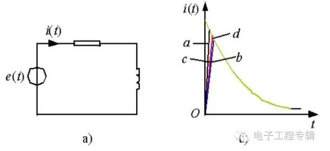
Figure 2 Responsive wave shapes of narrow pulses with the same impulses
Replaced by a series of pulses of equal bands of varying widths, a half-wave, half-width of the sine, which is seen as a series of N-connected pulses with equal widths, but varying in widths; replaced by a rectangular pulse, with equal bands of varying widths, a meso-point overlap, an equal area (fractions) and a change in width by the normal string pattern.
SPWM waveform - PWM waveforms with the same effect as a sine wave, depending on the pattern of the pulse width.
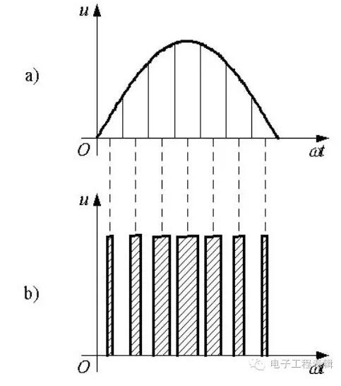
Figure 3 Using PWM wave instead of sine half wave
To change the equivalent output swirl range, change the pulse width at the same rate.
PWM current wave: The current-type reverse circuit is controlled by PWM, and it's the PWM current wave.
The PWM waveform can be equivalent to various waveforms:
DC chopper circuit: equivalent DC waveform
SPWM wave: Equivalent sine waveforms can also have the equivalent of other required waveforms, such as the non-sine exchange waveforms required for the equivalent effect, which have the same rationale as SPWM controls and are based on the equivalent area principle.
With the development of electronic technologies, a variety of PWM technologies have emerged, including: phase voltage Control PWM, Pulse PWM, Random PWM, SPWM, Wirevoltal Control PWM etc. This paper describes the pulse PWM method used in smart chargers for nickel-hydrogen batteries. It is a pulsing column with an equal pulse width as a PWM wave shape, which can be adjusted by changing the cycle of the pulse column, changing the width of the pulse or the space ratio, and adjusting the voltage to the frequency by applying appropriate control methods. The purpose of controlling recharge currents can be achieved by adjusting the PWM cycle and the PWM space ratio.
Specific application of PWM technology
PWM software method controls charging current
The basic idea of this method is to adjust the PWM ratio by using the PWM port of a single machine, without altering the PWM wave cycle, by adapting the PWM control register of the single machine to control the chargeable currents. The single machine required by this method must have both the ADC port and the PWM port as necessary, and ADC has the highest possible number of bits and the single machine works as quickly as possible. Before adjusting charged currents, single-piece machines quickly read the size of charged currents, then compare the default charge currents with those actually read, adjust the PWM ratio in the direction of increasing recharge currents if the actual currents are small, and adjust the PWM ratio in the direction of reducing charge currents if the actual currents are large. In adjusting the software PWM, care should be taken of the texture interference introduced by ADC, such as reading deviations and power work voltage, and the rational use of digital filtering techniques such as arithmetical averages. The software PWM has the following advantages and disadvantages.
PWM hardware circuits have been simplified and the cost of hardware reduced. Using software PWM, which does not use external hardware PWM and voltage comparators, it needs only a meta-measured device such as power MOSFET, continuous magnetic cores, and energy storage capacity, which greatly simplifys the peripheral circuits. It controls the size of the trickle-down. In the PWM-controlled charging process, a single machine can detect in real time the size of the chargeable current at the ADC port and determine the direction of PWM ' s contribution to the space. Batteries wake up. A single-piece machine can set the size of the chargeable current at any time using the ADC port and PWM repository. So, for batteries with lower battery voltage, the battery can be recharged for a period of time, and in the case of small currents, it can be considered constant, with less damage to the battery.
The current control accuracy is low. The perception of the size of charged currents is achieved by the current sample resistance, which is transmitted to the input ADC port of the single machine, where the voltage of a single machine reads the current of charge. If the sample resists are set at Rsample (in ounces), the sample resists at Vsample (in mV) and the 10-bit ADC reference voltage is 5.0V. A 5 mV is converted to a current value of 50 mA, so the software PWM has a maximum current control accuracy of 50 mA. If you want to increase the current control accuracy of the software PWM, you can try to reduce the reference voltage of ADC or use more than 10 ADC single-formula machines.
PWM is soft-started. In the process of running large current rapid charging, charging from stop to restart, because of the anti-electric dynamics on the magnetic core, it is necessary to reduce the effective empty ratio of PWM when recharging, in order to overcome the problem of uncontrollable currents due to the slowness of software adjustments to PWM. Charges are not very efficient. When charged quickly, the actual time to stop charging or to slow up small currents is greater because of the application of charging software and the slow adjustment of the single machine ' s PWM. In order to overcome the low recharge efficiency associated with shortcomings 2 and 3, we can use charging times that are longer, while charging times are shorter, e.g. charge time of 2s 50 ms, plus 50 ms at the slow start of the current at soft start, set at 50 ms, with a real charge efficiency of (2000m-100ms)/2000ms = 95%, which also ensures recharge efficiency of more than 90%.
Since the frequency of the operation of single machines is generally around 4 MHz, the work of PWM produced by single machines is low, and the time required for single machines to read charged currents in the ADC mode, the frequency of charging currents is relatively low with the software PWM, which can be controlled by external high-speed PWM methods to overcome the above deficiencies. The PWM control chips now used in smart chargers are mainly such as TL494, which can work at a frequency above 300 kHz, plus resistance elements, which can perform constant flow-restrictive pressure on battery charging, with only one common I/O port to control TL494 energy. The following advantages and disadvantages can also be used to replace TL494, e.g. LM393 and LM358, with a voltage comparison. The current is highly accurate. The control accuracy of charged currents is only related to the accuracy of the current sample resistance, and is not related to the single machine. It is not subject to the adjustment speed of the software PWM and the accuracy of ADC. Charge efficiency is high. There is no slow start of the software PWM, so during the same constant current charge and the same charge time, the energy in the battery is high. Because of the relatively stable currents and very small fluctuations during charging, the impact on batteries is small, and TL494 has a restraining effect that can protect batteries well. Hardware is more expensive. The use of TL494 adds to the cost of products, which can be overcome by LM358 or LM393.
Trickle-down controls are simple and pulsive. When batteries are charged, they are usually charged in the form of trickle-down charges to overcome the volume loss associated with the battery's self-discharge effect. The normal I/O control port for a single machine does not function as a PWM port, even if simple PWM functionality can be achieved using software simulations, but because the real-time nature of the work of a single machine requires a lower PWM frequency of software simulations, the final method is a pulse charge, e.g. 10 per cent of the time is charged, and no charge is applied for 90 per cent of the time.
For the pulsation of a simple hardware PWM trickle-down charge, a single machine with a PWM port can be used to address the pulsation of the trickle-off by combining the external PWM chip. This can be done to control the charge-down current: when a constant large current is rapidly charged, the PWM of a single machine can be exported to high level (PWM control chip high level power) or low level power (PWM control chip low level power); When a trickle-down charge is made, the PWM control port of the single machine can be exported to the PWM signal and the PWM ratio can then be adjusted by testing the pressure reduction on the electrical resistance of the current sample to meet the requirements.
The PWM generally selects the voltage Control Reverser to change the frequency of the reverse transistor output waveform by changing the time of power transistor interconductor, and the break time ratio of the transistor tube every half-cycle, i.e. by changing the size of the voltage side of the output of the reverser by changing the pulse width.
The whole flow is largely symmetrical with the reverse.
In short, the final output wave shape can be adjusted, the by-product values can be adjusted, and even the power factor can be adjusted, although it appears that the sine waves are used as the base wave.
For example, Microchip's PIC16C67 contains two PWM controllers, each of which can choose the time and time of connection. The space ratio is the ratio of the time of connection to the cycle; the change frequency is the penultimate of the cycle. Before the PWM operation, the microprocessor requires the following tasks to be performed in the software:
:: Sets the timer/calculator on the film that provides the modem wave
:: Set up access time in the PWM control register
:: Set the direction of the PWM output, which is a universal I/O tube foot
* Start timer
* Enable PWM controller
While specific PWM controllers differ in programming details, their basic thinking is usually the same. One advantage of communication and control PWM is that the signal from the processor to the accused system is in digital form, without the need for a numerical simulation. Increased resistance to noise is another advantage of PWM vis-à-vis analogue control, and this is the main reason why PWM is used for communication at some point. Moving from analogue signals to PWM can significantly increase communication distance. At the receiving end, high-frequency square waves can be filtered out through appropriate RC or LC networks, and signals restored to analogue. PWM is widely used in multiple systems. As a concrete example, we look at a brake that uses PWM control. In short, brakes are a device that binds something. Many brakes use analogue input signals to control the size of the plugged pressure (or brake power). The greater the voltage or current on the brake, the greater the brake pressure. The output of the PWM controller can be connected to a switch between the power supply and the brake. To generate greater brake power, it is only necessary to increase the empty ratio of PWM output through software. If a brake pressure of a given size is to be generated, measurement is required to determine the mathematical relationship between the space ratio and the pressure (the formula or search table of the result is modified to control temperature, surface wear, etc.).
Assuming, for example, that the pressure on the brake is set at 100 psi, the software will conduct a reverse search to determine what the weight of the pressure of this size should be. Then the PWM space ratio will be set to this new value, and the brakes will respond accordingly. If there is a sensor in the system, the ratio can be adjusted by closed loop control until the required pressure is accurately generated. In sum, PWM is both economical, space-efficient and noise-resistant and an effective technology that is worthy of being used by a wide range of engineers in many design applications.
- 2 Thermistor algorithm:
Working principle:
Thermal sensitivity resisters are the category of sensitive elements, which are classified according to temperature coefficients as thermal sensitivity resisters (PTCs and NTCs). Thermal sensitivity resisters are typically characterized by sensitivity to temperature and display of different electrical resistance values at different temperatures. The positive temperature factor thermal sensitivity resisters (PTCs) are larger when temperatures are higher and the negative temperature factor thermal sensitivity resisters (NTCs) are lower when temperatures are higher, and they are part of the semiconductor units.
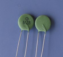
Thermal sensitivity resistance will remain inactive for a long time; when ambient temperatures and currents are in zone c, the heat-sensitive resistance has a dissipation power close to the heat-generation power, so that it may also be inactive. Thermal sensitivity resistance, at the same ambient temperature, is dramatically reduced by the increase in currents; thermal sensitivity resistance has shorter motion time and smaller maintenance and movement currents at relatively high ambient temperatures.
- The ptc effect is a ptc effect, i.e. a positive temperature coefficient effect, which simply means that the electrical resistance of this material increases with the temperature. For example, most metal materials have ptc effects. In these materials, the ptc effect is a linear increase in electrical resistance with temperature, which is commonly referred to as the linear ptc effect.
- Non-linear ptc effects can be seen in materials that vary dramatically increasing several to a dozen orders of magnitude along narrow temperatures, i.e., the non-linear ptc effect, which can be seen in a number of types of conductive polymers, such as high-molecular ptc thermal sensitivity resistance. These conductive polymers are very useful for the manufacture of electrical current protection devices.
- High Molecular ptc thermal sensitivity electrical resistance is used to protect overflow High Molecular ptc thermal sensitivity resistance is often referred to as self-rehabilitation fuse (hereinafter referred to as heat sensitivity resistance) and is therefore well suited to be used as an overflow protection device because of its unique positive temperature coefficient electrical resistance. The use of heat-sensitive electrical resistance is, like common fuses, used in a series of circuits.
When the electrical circuit works normally, heat-sensitive resistance temperatures are close to room temperature and the electrical resistance is very small, and the chain does not prevent the passing of electricity through the circuit; and when the electrical circuit passes through a malfunction, heat-sensitive resistance increases the temperature as a result of increased heat power, and when the temperature exceeds the temperature of the switch (ts, see figure 1), the electrical resistance increases dramatically and the currents in the circuit rapidly decrease to safety ... Changes in electrical currents during the protection of the communication circuit for heat-sensitive electrical resistance. The heat-sensitive electrical resistance is followed by a significant reduction in electrical currents in circuits, and the t-time of the heat-sensitive electrical resistance is shown in the diagram. Because high-molec ptc heat-sensitive resistance is well designed, it can be adjusted to temperature sensitivity by changing its own switch temperature (ts) and thus can function both as temperature protection and overflow protection, such as the Kt16-1700dl specification of heat-sensitive electrical resistance, which is applied to the overflow and over-temperature protection of lithium-ion and nickel-hydrogen batteries due to low movement temperatures. The effect of ambient temperatures on high-molec ptc heat-sensitive electrical resistance The high-molec ptc heat-sensitive electrical resistance is a direct-heat, step-trip heat-sensitive electrical resistance that is associated with its own heat and heat-dissemination processes, so that its currents (ihold), motion currents (itrip) and motion time are influenced by ambient temperature. When ambient temperatures and currents are in a region, thermal-sensitized heat-retardation power is greater than the dissemination power; When ambient temperatures and currents are in zone b, heat power is less than dispersing power, high-molec ptc thermal sensitivity resistance can be reused because resistance can be restored, so it can be repeated repeatedly. Figure 6 shows the pattern of time-sensitive resistance during recovery. Resumes generally return to levels around 1.6 times the initial value in 10 to dozens of seconds, at which point the maintenance of heat-sensitive electrical resistance is restored to a rated value and can be used again. The recovery of heat-sensitive resistance in size and thickness is relatively rapid; The recovery of heat-sensitive resistance, both in size and thickness, has been relatively slow.
Basic features:
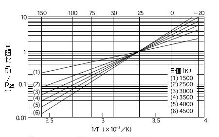
The electrical resistance-temperature properties of heat-sensitive electrical resistance can be approximated in the following form: R=R0exp{B(1/T-1/T0)}: R: the electrical resistance value at temperature T(K), Ro: temperature T0, (K), B:B, *T(K)=t(oC)+273.15 In practice, the B value of heat-sensitive electrical resistance is not constant and varies by material composition, with a maximum or even 5K/°C. Therefore, there is some error between the application of Model 1 within a larger temperature range and the measured values. Here, if the B value in Model 1 is calculated as a function of temperature as indicated in Model 2, the error between the measured values can be reduced and considered to be approximately equal.
BT = CT2+DT+E, above which C, D, and E are constants. In addition, fluctuations in B values due to different production conditions cause constant E to change, but constants C, D remain unchanged. Therefore, when looking at B-value fluctuations, only constant E is considered. For constant C, D, E, constant C, D, E can be 4-point (temperature, electrical resistance) data (T0, R0). (T1, R1). (T2, R2) and (T3, R3), calculated by 3-6. First, model 3 draws B1, B2, B3 from T0 and T1, T2, T3, and then replaces the following.
An example of a resistance value is given for a test with a resistance value of 5 (k) at 25 °C and a heat-sensitive resistance value of 50 (K) at 10 °C ~ 30 °C. Step 1 is a constant of C, D, E. To = 25 + 273.15 T1 = 10 + 273.15 T2 = 20 + 273.15 T3 = 30 + 273. 15(2) for BT = CT2+DT+E+50. (3) for R = 5exp {(BT1/T-1/298.15)}, for R.*T: 10+ 273.15 ~ 30+ 273.15.
NTC thermal sensitivity resistance is a temperature sensor that is widely used because of their low cost and availability in many sizes and shapes. Using modern microcontrollers, it is now easy to program the above equations and obtain direct readings (°C (or any other temperature unit) without the need for sophisticated analogue linear circuits.
Some of the other disadvantages that should be mentioned: first, the work temperature range is limited to about -50 to +150°C. This, of course, depends on the specific NTC model, but these limitations cannot be exceeded because most 103F heat-sensitive NTC uses silicon.
NTC thermal sensitivity resistance is usually calibrated by the plant: actual R 25 and B 25/100 can change from one NTC to another and always require some kind of circuit adjustment to make absolute temperature readings.
Finally, by using NTC as a temperature sensor, as currents heat up 10K3435NCC and introduce measurement errors, large currents should be avoided as much as possible. Therefore, high NTC values (more than 10k) are better for thermometers. Small NTCs are not usually used as temperature sensors, but they make very good wave current limiters. 100 K3950 NTC was initially cold when NTC’s connected circuits were connected, providing several instances of electrical resistance, limiting current surges and preventing fuses from melting. Once the currents began to flow, NTC’s heat-sensitive electrical resistance increased, and its electrical resistance fell within the m range, leaving the main current undisturbed.
Technical parameters:
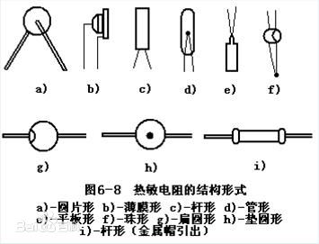
1 Marked Resistance Rc: Generally refers to the actual electrical resistance value of the heat-sensitive resister at 25°C. 2 Actual resistance value RT: taken at a given temperature
The measured resistance value.
Material constant: It is a parameter that describes the physical properties of heat-sensitive electrical resistance material, and it is also a heat-sensitization indicator. The greater the B value, the greater the sensitivity of the heat-sensitive resistor. It should be noted that, in practice, the B value is not a constant, but increases slightly with temperature.
4 Resistance temperature factor αT: It represents the resistance rate at 1°C, in %/°C.
Five-time constant: The heat-sensitive electrical resistor is a heat-deliberate, time-consistent, a parameter that describes the heat-resistor inertia. It is defined as the temperature of the heat-sensitive resistor changes the time of 63.2 per cent of the difference between two specific temperatures when the temperature changes suddenly from one specific temperature to another in a state of inefficiency. The smaller, the smaller the heat-resistor is the smaller.
PM: Under the prescribed technical conditions, the heat-sensitive electrical retardant shall not exceed the rated power at the time of its actual use. If the heat-sensitive electrical resistor works at an ambient temperature above 25°C, the load shall be reduced accordingly.
7 Standard working current IM: Thermally sensitive electrical resisters are given nominal current values under working conditions.
Measured Pc: Thermally sensitive electrical retardants at specified ambient temperatures are subject to a resistance value of not more than 0.1% consumed when they are heated by the test current.
Thermistor
Thermistor
Maximum voltage: For NTC Thermal Sensitive Resistor, it is the maximum direct current voltage allowed to be applied continuously at specified ambient temperatures without causing heat-sensitive resistor to lose control; for PTC Thermal Sensitive Resistor, it is the maximum direct current voltage allowed to be applied continuously on the thermosensitive resistor at specified ambient temperatures and static air, and it is guaranteed that thermally sensitive resistor will function normally at the maximum direct current voltage in the properties of the PTC. Tmax: The maximum temperature allowed for the long-term continuous operation of the heat-sensitive resister under prescribed technical conditions.
(11) Switch temperature tb: The temperature of the PTC thermal sensitivity resistor at which the electrical resistance value begins to increase.
Dift factor H: Thermal sensitivity resisters consume power at 1 °C, in mW/°C.
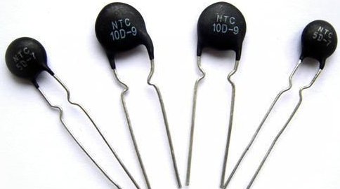
NTC Heat-sensitive resist temperature calculation formula Rt = R *EXP (B*(1/T1-1/T2))
T1 and T2 here refers to K degrees, Kelvin temperature, K degrees = 273.15 (absolute temperature) + degrees Celsius;
Where T2 = (273.15 + 25) Rt is the heat-sensitive barrier at T1 temperature;
R is the nominal resistance of heat-sensitive electrical resistance at T2 constant temperature;
The B value is an important parameter of the thermistor;
EXP is the nth power of e;
Conversion to: 1/T1 = inn (Rt/R)/B+1/T2, TI, minus 273.15 is the actual temperature, and error correction of +0.5.
Program:
#include "math.h"
const float Rp=10000.0; //10K
const float T2 = (273.15+25.0); //T2
const float Bx = 3950.0; //B
const float Ka = 273.15;
float temp;
while(1)
{
temp = 1/(log(Rt/Rp)/Bx + (1/T2));
temp = (temp - Ka + 0.5)*10;
LCD ShowxNum (86,150,temp, 5,16,0x80) // Show temperature
}
The steps are broken down as follows:
float Get_Temp(void)
{
float Rt;
float temp;
Rt = Get TempRESTOR(); / /get the resistance value
//like this R=5000, T2=273.15+25,B=3470, RT=5000*EXP(3470*(1/T1-1/(273.15+25)),
temp = Rt/Rp;
temp = log(temp);
//ln(Rt/Rp)
temp/=Bx;
//ln(Rt/Rp)/B
temp+=(1/T2);
//ln(Rt/Rp)/B+(1/T2)
temp = 1/(temp);
temp-=Ka;
temp+=0.5;
//Add 0.5 error correction
return temp;
}
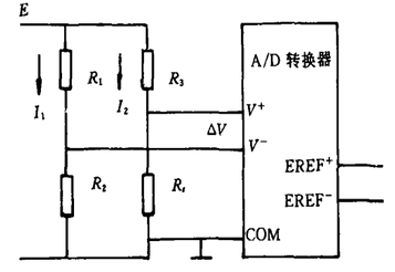
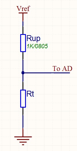
In embedded systems, heat-sensitive electrical resistance is often used to test temperature. Its circuits are typically used for electrical decomposition circuits and AD conversions, and temperature data can be obtained by measuring the value of "To AD".
- The relationship between heat-sensitive resistance and temperature is linear. We need to know the relationship between resistance and temperature first, assuming that:
Rt=K*t+B (0)
t=(Rt-B)/K (1)
The K.B. here is the coefficient of the Rt(t) straight equation. There are two unknowns.
Resist - Temperature Data Sheets for heat-sensitive resistance, randomly searching for two t1 and t2 and corresponding electrical resistance values within the temperature of our concern...
In formula, we have to bring an equation that solves it, and we can get K and B. If you find this resistance-- the temperature table is not linear enough, you can construct a function using a non-linear interpolation method (e.g., the LaGrandian or parabolic interpolation values, etc., are simple and efficient).
So we already know K and B or Rt(t) functions, so let's just say, just know the temperature. We can calculate the current resistance value, and vice versa.
- Back to the top circuit, apparently AD = Rup/(Rup+Rt) - > Rt = Rup * AD/(1023-AD)// If 10 ADs are used, the maximum is 1023 (2)
Bring (2) into (1)
t=(Rup*AD/(1023-AD)-B)/K
This way, the current temperature can be calculated directly from AD results.
Interface Design
JDY-08 Bluetooth module functional principle:
The JDY-08 extremity module is based on the Bluetooth 4.0 protocol standard with a working frequency range of 2.4 GHZ and is based on GFSK, with a maximum launch power of 0db and a maximum launch distance of 80 m, using the TICC2541 chip design to support the user in changing the name of the device through AT commands and to serve UUID, launch power, matching passwords, etc., to facilitate quick and flexible use.
2. Technical parameters:
- Communication rate 3Kbytes/second
- Serial support for 1024Bytes writing during APP pass-through
- Effective communication distance 15 to 30 meters
- Support PWRC pin to control sleep
- supports IO port control disconnection
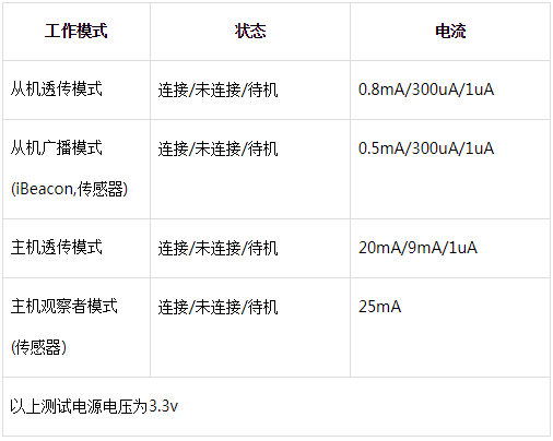
Broadcast current setting
The default broadcast interval is the smallest, and because of the product requirements of different users, there is a great deal of demand for the cost of the product, so we...
This is also taken into account in the module, where broadcast interval is set by AT command
The default broadcast interval is: AT+ADVIN 0 is 100 ms
Use AT+ADVIN to set broadcast intervals when users need to have some power requirements
AT command Broadcast time Current
AT+ADVIN 0 100ms 0.6mA
AT+ADVIN 1 500ms 0. 1mA
AT+ADVIN 2 750ms 0. 05mA
AT+ADVIN 3 1000ms 0. 02mA
The above is set by AT command, and the user can set the broadcast interval by mobile phone, but not the longer the broadcast interval.
Well, it's too long for the radio to affect the connection time. It takes a long time to connect to the cell phone, setting up 100 or 500 ms.
It's about the right and the left. Sensor applications can be a little longer, because there's no need to connect.
Connection interval setting
The current of the user when connected to the cell phone can be set, either by AT command or by mobile phone
The AT command settings can be set by: AT+NEIN
AT command Broadcast time Current
AT+NEIN0 10ms 0. 8mA
AT+NEIN1 100ms 0. 2mA
AT+NEIN2 500ms 0. 05mA
The above is the connection interval set by AT command, and the user can also set the connection interval by mobile phone, not the connection interval
The longer the settings, the better they are, the better they depend on the user's view.
The default interval is usually required, if only for some control applications, or small data should be, and the connection interval is set
longer.
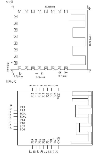
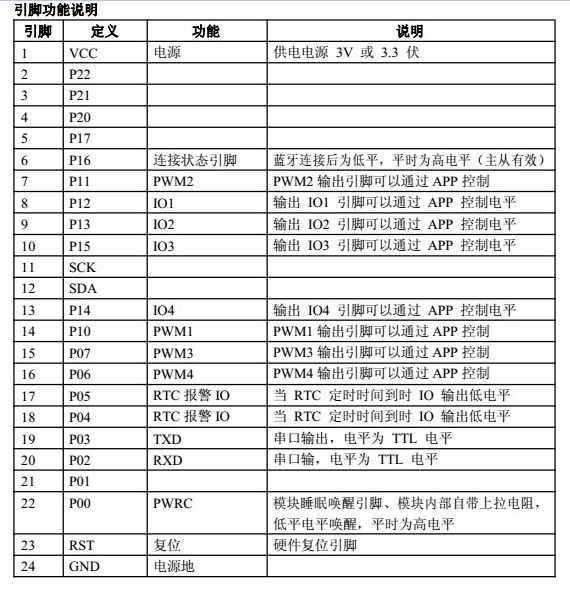
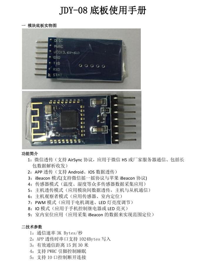
Function usage of PWM:
First step to set the PWM frequency 250HZ (frequency range 50 - 4KHZ)
AT command: AT+PWMFRE 250 returns OK
Second step to open PWM
AT command: AT+PWMOPEN 1 returns OK (1 is open or not PWM, 2 is open)
Step 3 opens the pulse width set for PWM (with the output of PWM on the 4th road, so you can set the PWM pulse width on the 4th road)
AT command: AT+PWM1PUS90 returns OK which indicates a pulse width of 90% setting PWM1
AT Directive: AT+PWM2PUS 10 returns OK which indicates a pulse width of 10% setting PWM2
The fourth step users can read the PWM working state
AT command: AT+PWMPUS returns status, see manual
The fifth step is to turn off the PWM function
AT Instruction: AT+PWMOPEN 0 so that the module shuts down the PWM function, and if the PWRC leads to a high level of power, the module goes into low-capacity mode.
* Activity for scanning and displaying available Bluetooth LE devices.
*/
public class DeviceScanActivity extends ListActivity {
private LeDeviceListAdapter mLeDeviceListAdapter;
private BluetoothAdapter mBluetoothAdapter;
private boolean mScanning;
private Handler mHandler;
private static final int REQUEST_ENABLE_BT = 1;
// Stops scanning after 10 seconds.
private static final long SCAN_PERIOD = 10000;
@Override
public void onCreate(Bundle savedInstanceState) {
super.onCreate(savedInstanceState);
getActionBar().setTitle(R.string.title_devices);
mHandler = new Handler();
// Use this check to determine whether BLE is supported on the device. Then you can
// selectively disable BLE-related features.
if (!getPackageManager().hasSystemFeature(PackageManager.FEATURE_BLUETOOTH_LE)) {
Toast.makeText(this, R.string.ble_not_supported, Toast.LENGTH_SHORT).show();
finish();
}
// Initializes a Bluetooth adapter. For API level 18 and above, get a reference to
// BluetoothAdapter through BluetoothManager.
final BluetoothManager bluetoothManager =
(BluetoothManager) getSystemService(Context.BLUETOOTH_SERVICE);
mBluetoothAdapter = bluetoothManager.getAdapter();
// Checks if Bluetooth is supported on the device.
if (mBluetoothAdapter == null) {
Toast.makeText(this, R.string.error_bluetooth_not_supported, Toast.LENGTH_SHORT).show();
finish();
return;
}
}
@Override
public boolean onCreateOptionsMenu(Menu menu) {
getMenuInflater().inflate(R.menu.main, menu);
if (!mScanning) {
menu.findItem(R.id.menu_stop).setVisible(false);
menu.findItem(R.id.menu_scan).setVisible(true);
menu.findItem(R.id.menu_refresh).setActionView(null);
} else {
menu.findItem(R.id.menu_stop).setVisible(true);
menu.findItem(R.id.menu_scan).setVisible(false);
menu.findItem(R.id.menu_refresh).setActionView(
R.layout.actionbar_indeterminate_progress);
}
return true;
}
@Override
public boolean onOptionsItemSelected(MenuItem item) {
switch (item.getItemId()) {
case R.id.menu_scan:
mLeDeviceListAdapter.clear();
scanLeDevice(true);
break;
case R.id.menu_stop:
scanLeDevice(false);
break;
}
return true;
}
@Override
protected void onResume() {
super.onResume();
// Ensures Bluetooth is enabled on the device. If Bluetooth is not currently enabled,
// fire an intent to display a dialog asking the user to grant permission to enable it.
if (!mBluetoothAdapter.isEnabled()) {
if (!mBluetoothAdapter.isEnabled()) {
Intent enableBtIntent = new Intent(BluetoothAdapter.ACTION_REQUEST_ENABLE);
startActivityForResult(enableBtIntent, REQUEST_ENABLE_BT);
}
}
// Initializes list view adapter.
mLeDeviceListAdapter = new LeDeviceListAdapter();
setListAdapter(mLeDeviceListAdapter);
scanLeDevice(true);
}
@Override
protected void onActivityResult(int requestCode, int resultCode, Intent data) {
// User chose not to enable Bluetooth.
if (requestCode == REQUEST_ENABLE_BT && resultCode == Activity.RESULT_CANCELED) {
finish();
return;
}
super.onActivityResult(requestCode, resultCode, data);
}
@Override
protected void onPause() {
super.onPause();
scanLeDevice(false);
mLeDeviceListAdapter.clear();
}
@Override
protected void onListItemClick(ListView l, View v, int position, long id) {
final BluetoothDevice device = mLeDeviceListAdapter.getDevice(position);
if (device == null) return;
final Intent intent = new Intent(this, DeviceControlActivity.class);
intent.putExtra(DeviceControlActivity.EXTRAS_DEVICE_NAME, device.getName());
intent.putExtra(DeviceControlActivity.EXTRAS_DEVICE_ADDRESS, device.getAddress());
if (mScanning) {
mBluetoothAdapter.stopLeScan(mLeScanCallback);
mScanning = false;
}
startActivity(intent);
}
private void scanLeDevice(final boolean enable) {
if (enable) {
// Stops scanning after a pre-defined scan period.
mHandler.postDelayed(new Runnable() {
@Override
public void run() {
mScanning = false;
mBluetoothAdapter.stopLeScan(mLeScanCallback);
invalidateOptionsMenu();
}
}, SCAN_PERIOD);
mScanning = true;
mBluetoothAdapter.startLeScan(mLeScanCallback);
} else {
mScanning = false;
mBluetoothAdapter.stopLeScan(mLeScanCallback);
}
invalidateOptionsMenu();
}
// Adapter for holding devices found through scanning.
private class LeDeviceListAdapter extends BaseAdapter {
private ArrayList<BluetoothDevice> mLeDevices;
private LayoutInflater mInflator;
public LeDeviceListAdapter() {
super();
mLeDevices = new ArrayList<BluetoothDevice>();
mInflator = DeviceScanActivity.this.getLayoutInflater();
}
public void addDevice(BluetoothDevice device) {
if(!mLeDevices.contains(device)) {
mLeDevices.add(device);
}
}
public BluetoothDevice getDevice(int position) {
return mLeDevices.get(position);
}
public void clear() {
mLeDevices.clear();
}
@Override
public int getCount() {
return mLeDevices.size();
}
@Override
public Object getItem(int i) {
return mLeDevices.get(i);
}
@Override
public long getItemId(int i) {
return i;
}
@Override
public View getView(int i, View view, ViewGroup viewGroup) {
ViewHolder viewHolder;
// General ListView optimization code.
if (view == null) {
view = mInflator.inflate(R.layout.listitem_device, null);
viewHolder = new ViewHolder();
viewHolder.deviceAddress = (TextView) view.findViewById(R.id.device_address);
viewHolder.deviceName = (TextView) view.findViewById(R.id.device_name);
view.setTag(viewHolder);
} else {
viewHolder = (ViewHolder) view.getTag();
}
BluetoothDevice device = mLeDevices.get(i);
final String deviceName = device.getName();
if (deviceName != null && deviceName.length() > 0)
viewHolder.deviceName.setText(deviceName);
else
viewHolder.deviceName.setText(R.string.unknown_device);
viewHolder.deviceAddress.setText(device.getAddress());
return view;
}
}
// Device scan callback.
private BluetoothAdapter.LeScanCallback mLeScanCallback =
new BluetoothAdapter.LeScanCallback() {
@Override
public void onLeScan(final BluetoothDevice device, int rssi, byte[] scanRecord) {
runOnUiThread(new Runnable() {
@Override
public void run() {
mLeDeviceListAdapter.addDevice(device);
mLeDeviceListAdapter.notifyDataSetChanged();
}
});
}
};
static class ViewHolder {
TextView deviceName;
TextView deviceAddress;
}
}
The JDY-08 module exits are defaultly configured for transhipment, and generally defaults are for transhipment, if required.
If the sensor function is used, the client must follow the instructions or notes before purchasing it.
This chapter only addresses the AT command configuration for sensor functions in a functional mode that is relevant after purchase
The module connects the USB trans-string or the MMU serial (RXD, TXD), by the cross-linking of the serial, sending with the serial port
When commanding, direct the PWRC of the module to the ground and connect to the power of the module (VCC, GND) with a power pressure of 3.3 V
or 3V
Once we're done with that line, we'll start talking about what's going on in AT.
Step 1: Configure modules to iBeacon mode
Note that sensor functions are only applied in iBeacon mode and therefore need to be configured to iBeacon mode
Send by serial: AT+HOSTEN3 returned: OK
Step 2: Restart the module
Sending via serial: AT+RST for reverting
Step 3: Set the temperature value to 33 degrees
Sending via serial: AT+TEMP33 returns: OK
The fourth step: Set the humidity value to 11%
Send by serial: AT+HUMID11 back OK
Step 5: Set the sensor to 90% power.
Send via serial: AT+BATT90 returns OK
Because the sensor function is based on the iBeacon application, if you have a large number of sensors, the commands of the two sensors above
You can use iBeacon's instructions to transmit your sensor data if it doesn't satisfy your product application.
AT+STRUID+32-bit string length, note this 32-bit data format is: a hexadecimal string
AT+MAJOR +4-bit string length, string formatted as: hexadecimal string
AT+MINOR+4-bit string length. String formatted as: Hexadecimal string
When users need to judge their own equipment on AP, configure the manufacturer ID
General Bluetooth-based equipment can be judged by Bluetooth service UUID and device name, but these can all be
It's the same because our standard module Bluetooths are the same.
Also, we have added the manufacturer's ID function for the app to recognize home-based equipment.
Configurer ID value: 65330 (decimal value) and hexadecimal value: 1985
Send by serial: AT+VID1985 returns: OK
Main communication from the Bluetooth module refers to two Bluetooth modules that communicate with each other, one as a host and one as an operator, and they communicate with each other.
Letter, the first module is the machine module, the second module is the host module
The first step is to power on the host and slave modules
and connect the module to the USB or MMU and note that the chain of entry is cross-cutting
, start AT command debugging after connection
Step two, open the first module from the machine, open it from the machine by default, and also by sending AT+ADVEN1
to open the broadcast
Step 3: Set the command of the main module
1) Set the module to host pass mode, return OK means settings are complete
Send command: AT+HOSTEN1 returns OK
2) Set module to restart
Send: AT+RST
3) Scan peripheral BLE commands
Send: T+SCAN1 Return OK
4) Number of BLE bluetooths read (up to 8 scanners)
AT+GETDCD returns DEV 1: means scanned to a device
5) Machine MAC address (0-7) to read scanning lists
Send: AT+RSLV0 returns: MAC:e3435480
6) Connect to scan list 0 device (0-7)
Send: AT+CONNET0
You can also connect directly from the MAC address to: AT+CONNET1122233445566
112233445566 is the MAC address of the flight.
7) Send a command to find out whether it is connected to the slave
Send: AT+GETSTAT returns: STS:11 means connected
8) Hardware determines whether it is connected to the slave machine
The 6 foot of module 6 is the lead for connectivity, which is successfully low and not high
9) When the mainframe is connected successfully, the data will be passed through.
The module connects the USB trans-string or the MMU serial (RXD, TXD), by the cross-linking of the serial, sending with the serial port
When commanding, direct the PWRC of the module to the ground and connect to the power of the module (VCC, GND) with a power pressure of 3.3 V
or 3V
Once we're done with the above line, we'll start talking about the operation of the AT command.
Step 1: Configure the module to host observer mode
Send by serial: AT+HOSTEN2 back: OK
Step 2: Restart the module
Sending via serial: AT+RST for reverting
Through the above settings, the module has been configured as the host observer mode, at which point the host begins to receive data from the machine sensors,
The format of sensor data received by the host serial port is as follows
Data format: 2 bytes) head + 6 (bytes) MAC + 1 (byte) RSSI + 2 (bytes) Mayor + 2 (bytes) Minor +
2(bytes)VID + 1(byte) TEMP + 1(byte) HUMID + 1(bytes)BATT
Users can identify their own sensor data via VID, then distinguish each sensor from the MAC address
Note: Data received from the host: MAJOR, MINOR, VID, TEMP, HUMID, BATT are sent from the machine
Data sent by AT command in sensor mode
AT+MAJOR000A
AT+MINOR0007
AT+VID6677
AT+TEMP44
AT+TEMP44
AT+ BATT90